Friday, 05 February 2016
A cost-effective method for mass production of printed flexible graphene-based electronic devices
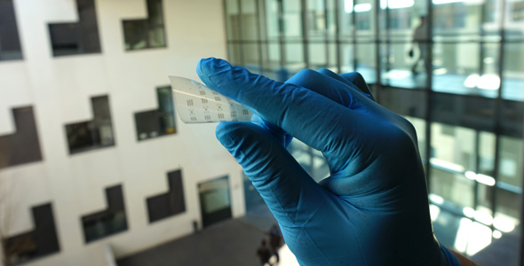
The ICN2 NanoBioelectronics and Biosensors Group, led by the ICREA Research Prof Arben Merkoçi, presents a versatile, low-cost and customizable method for patterning graphene oxide onto a myriad of substrates. The patented technique, published in ACS Nano, requires neither a clean room nor organic solvents. It consists of three easy steps: printing, filtering and pressing.

The introduction of flexible electronics meant a change of paradigm on established technologies. Now, the NanoBioelectronics and Biosensors Group at the Institut Català de Nanociència i Nanotecnologia (ICN2), a research center of the Barcelona Institute of Science and Technology (BIST), presents a versatile, low-cost and customizable method for patterning graphene oxide onto a myriad of substrates. This patented technique, published in the latest issue of ACS Nano, might also be appropriate for other electronic materials. The first author of the article is Luis Baptista-Pires, PhD student at the ICN2 Group led by the ICREA Research Prof Arben Merkoçi, who is the corresponding author of this work.
Some methods for patterning electronic devices involve long fabrication periods, high cost, great expertise and clean room facilities. Moreover, these methods are not versatile or effective for designing simple devices such as transistors or capacitors and overall biosensors that require effective linking of specific (bio)receptors. The patterning method by ICN2 allows the transfer of graphene oxide onto almost any substrate in an easy, cost-effective and customizable way.
The patented method consists of three steps:
- Printing: A nitrocellulose membrane is patterned onto the desired shape using a wax printer. The inverse pattern is printed onto the membrane surface.
- Filtering: The wax-printed membrane is set onto the filtering glass and the suspension of graphene oxide is filtered. The wax clogs the membrane pores wherever it is printed.
- Pressing: The pattern obtained is transferred by pressure to the desired target substrate.
This green, low-cost and versatile approach will enable in situ transfer of multiple electronic devices such as field effect transistors (FET), LEDs, electrodes, solar cells, biosensors or supercapacitors. It requires neither a clean room nor organic solvents. The wax-printed membranes have 50μm resolution, long-term stability and infinite shaping capability over a variety of substrates, including textile, paper, adhesive film or PET. Additionally, the technology can be implemented in a roll-to-roll hardware, speeding up the printing. It is also is promising for implementation in under-developed countries.
For further information: Download the patented technology Flyer
Article Reference:
Luis Baptista-Pires, Carmen C. Mayorga-Martínez, Mariana Medina-Sánchez, Helena Montón, and Arben Merkoçi. Water Activated Graphene Oxide Transfer Using Wax Printed Membranes for Fast Patterning of a Touch Sensitive Device. ACS Nano, 2016, 10 (1), pp 853–860. DOI: 10.1021/acsnano.5b05963

