Researchers from Georgia Institute of Technology and ICN2 Advanced Electron Nanoscopy Group have recently published an article in Nano Letters. They show an improvement made on the growth procedure of a semiconductor nanowire at subeutectic conditions using hydrogen. These results may have a positive effect on the CMOS technology.
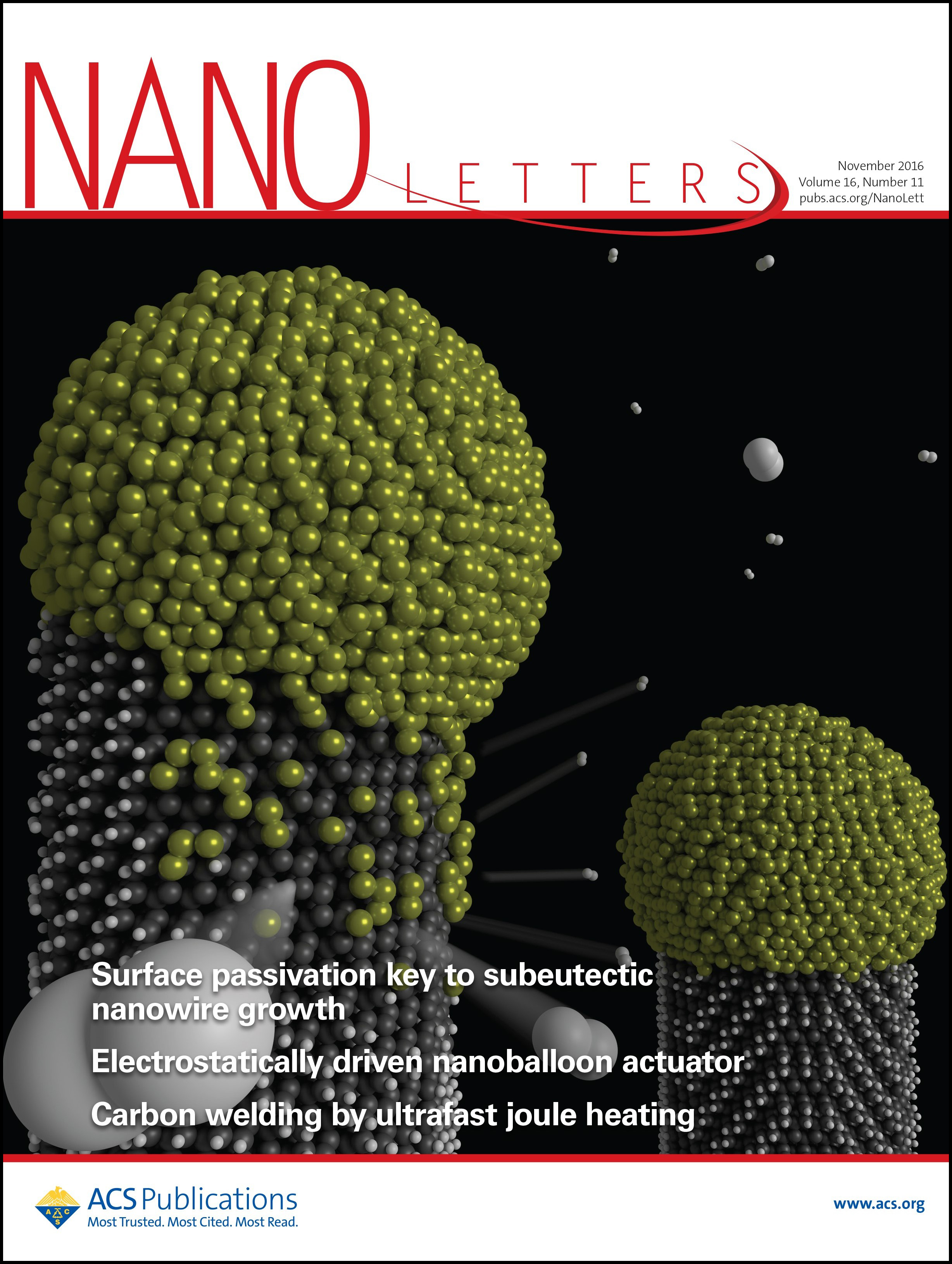
The front cover of the Nano Letters November issue is from a study developed by researchers that belong to Dr Michael Filler’s Group at the Georgia Institute of Technology, and to the ICN2 Advanced Electron Nanoscopy Group, headed by ICREA Research Professor Jordi Arbiol. The paper presented in the journal shows an improved procedure to enhance the growth of germanium nanowire. Hydrogen atoms adsorbed on the nanowire sidewall enable optimized subeutectic growth of the material. The CMOS (Complementary metal-oxide-semiconductor) technology could benefit from this new technique.
Nanoscience and nanotechnology play an important role on the creation and shaping of materials, using procedures such the following one. The growth of a germanium nanowire requires a catalytic material, liquid gold (yellow spheres), located in a medium full of Ge2H6 gas, an inorganic compound. The gold absorbs the germanium from the digermane until it reaches a saturation point. When the alloy saturates, the surplus atoms of germanium located inside the gold sphere precipitate to the base of the Au droplet. Repeating this process a germanium nanowire is created layer by layer. All procedures described in the article are performed below the eutectic temperature, at which the alloy at the catalyst droplet has the phase transition from liquid to solid.
However, the described technique has one big problem: some gold atoms may also precipitate together with the germanium ones through the sidewall meanwhile the creation of the nanowire is occurring (left structure in the cover image). It derives into two drawbacks. First, the gold may act as a deep-level trap for the charge carriers, thus limiting the device conductivity and its electronic performance. And second, if gold atoms fall from the droplet, it means the liquid sphere is continuously reducing its cross-section (tapering effect); it is important because the nanowire thickness depends on the droplet size. It is not optimal to have a nanowire that, along distance, has smaller radius and is covered by gold traps, decreasing its electronic properties.
These drawbacks have been recently amended by researchers from the Georgia Institute of Technology in collaboration with the ICN2 Advanced Electron Nanoscopy Group. Using hydrogen atoms, they are able to keep the gold together in the droplet, instead of falling on the sidewall along the process. The innovation on the procedure is to put hydrogen atoms (white) on the sidewall of the germanium nanowire (grey). Through the hydrogen created by the separation of the Ge2H6 and the external controlled addition, the researchers cover the surface of the nanowire with those hydrogen atoms. Thereby, gold does not fall (right structure in the cover image). Consequently, the germanium nanowire created has always the same thickness and keeps its purity, so its electrical characteristics are technologically relevant.
In the paper, the ICN2 Group devoted a great effort on the study of the atomically dispersion of gold atoms for different processes. They experimentally found the optimal conditions where electrical properties of the material were incremented, as a consequence of the non-fall of gold. The Advanced Electron Nanoscopy Group is internationally recognized in the nanowire growth field.
Currently, the majority of electronic circuits (microprocessors, memories, digital signal processors…) are developed using silicon, germanium or carbon. Before this work, these types of materials were hardly compatible with processes using gold as a catalyst. From now on, the CMOS, a technology for integrated circuits, could be improved due to the optimization of the creation of germanium (and also silicon) nanowires.
Article reference:
Saujan V. Sivaram, Ho Yee Hui, María de la Mata, Jordi Arbiol and Michael A. Filler. Surface Hydrogen Enables Subeutectic Vapor-Liquid-Solid Semiconductor Nanowire Growth. Nano Letters, 2016, 16 (11), Pages 6717-6723.
http://pubs.acs.org/doi/abs/10.1021/acs.nanolett.6b01640