Tuesday, 22 July 2025
ICN2 Researchers Discover New Properties of a Promising 2D Material for Electronics and Optoelectronics
These findings could be key to developing faster, more efficient, and flexible devices.
Transition metal dichalcogenides (TMDCs) are a class of materials that have been widely studied for potential use in electronic devices thanks to their excellent mechanical, optical and electrical properties. A notable example is molybdenum diselenide (MoSe₂), a two-dimensional (2D) layered material that has attracted considerable interest in recent years. However, to fully harness the potential of these materials and keep advancing the field, a deeper understanding of their charge transport properties is essential.
In this context, a team of researchers led by ICFO and ICN2, including Prof. Klaas-Jan Tielrooij (head of the Ultrafast Dynamics in Nanoscale Systems Group), studied the behaviour of electrical charges moving through MoSe₂ after it was irradiated with light. The results of the research, published in the journal Nature Communications, reveal new and unexpected insights into the electrical properties of these materials.
A Matter of Thickness
In this study, the researchers investigated how electric charges move through MoSe₂ crystals. Samples of varying thicknesses were analysed, down to a single atomic layer, revealing how the material’s thickness can dramatically affect its behaviour.
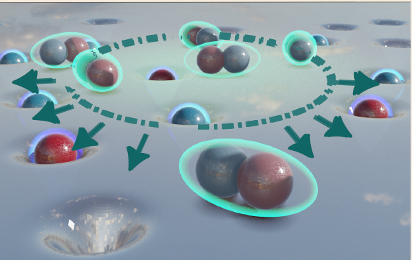
The study combined ultrafast microscopy experiments with advanced simulations, performed by collaborators at Marburg University in Germany, and revealed that electrons in the thinnest crystals (just one or two layers) undergo several distinct regimes of motion. In the earliest stages, the charges move extremely quickly and, within just a few picoseconds (one trillionth of a second), begin to form excitons, which are bound electron-hole pairs.
The researchers observed a surprising phenomenon known as negative diffusion when this happened: the charges within the excitons did not move in the usual direction — from regions with more charge to regions with less — but instead accumulated in already highly charged areas. Eventually, these excitons dissipate when they encounter defects in the material. Interestingly, this behaviour was not observed in thicker crystals, where only the first and last regimes occurred.
It was also observed that when the crystals were supported on a substrate, rather than suspended, their behaviour changed as well. In the supported case, the different transport regimes are much less well-defined. This highlights the crucial role that the thickness and the environment of the material play in determining how charges move through these systems.
In summary, this discovery provides a deeper understanding of the internal mechanisms and nanoscale phenomena affecting charge transport in TMDCs. Furthermore, this could be pivotal in designing future devices that are faster, more efficient, thinner and flexible, including sensors, transistors and future chips.
Reference article:
Lo Gerfo Morganti, G; Rosati, R; Brinatti Vazquez, GD; Varghese, S; Saleta Reig, D; Malic E; Van Hulst, NF; Tielrooij, KJ. Transient ultrafast and negative diffusion of charge carriers in suspended MoSe2 from multilayer to monolayer. Nature Communications. (2025). DOI: https://doi.org/10.1038/s41467-025-60197-3.