Thursday, 31 July 2025
ICN2 Researchers Envision How Optical Nanoscopies Could Shape the Future of Photonics with 2D Materials
ICREA Prof. Aitor Mugarza, Dr Marc G. Cuxart and Dr Emigdio Chávez-Angel contributed to the recently published Roadmap for Photonics with 2D Materials with a Chapter on the role of tip-enhanced nanoscopies in the atomic-scale study of light-matter interactions in these nanomaterials.
Photonics is just beginning to explore and use the special properties that 2D materials offer. They have unique properties that don't exist in their larger, bulk forms. Many of them have different and more complex electronic behaviors than the regular 3D materials.
The Atomic Manipulation and Spectroscopy Group, headed by ICREA Prof. Aitor Mugarza and represented by Drs. Marc G. Cuxart and Emigdio Chávez-Angel, together with field experts like Dr Pablo Merino from ICMM-CSIC, and Dr Martin Švec from the Institute of Physics of the Czech Academy of Science, have contributed to an article that presents the recent breakthroughs in photonics and 2D materials, identifies the current challenges and opportunities in the field, and explores multiple ways of meeting future goals through different topical chapters.
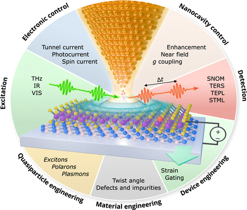
More specifically, Prof. Mugarza led a Chapter that zooms in on tip-enhanced nanoscopies, a family of characterisation techniques that will be implemented by ICN2 in the ALBA Synchrotron through the InCAEM project. Tip-enhanced nanoscopies work by placing a sharp metallic tip just about one nanometer above the surface of a material and illuminating the region with focused light. This creates a nanocavity, a tiny space where electromagnetic fields are amplified within volumes much smaller than the diffraction limit.
This allows the transfer of photons between the near- and far-field, enabling the transfer of photons from a laser to the nanoscale object, and from there to a detector.
The authors underline some future challenges, such as studying light−matter interactions in atomically engineered materials at the ultimate spatiotemporal limits of picometers and attoseconds, or expanding the ability to probe and control a wider range of quasiparticles at the nanoscale, beyond well-studied excitons and plasmons. While still in its early stages and facing several challenges, tip-enhanced techniques have already shown great potential. They could be key to advancing applications in fields like telecommunications, quantum information processing, theragnostics, and UV photochemistry.
Reference article:
Garcia de Abajo, FJ; Basov, DN; Koppens, FHL, et al. Roadmap for Photonics with 2D Materials. ACS Photonics. (2025). https://pubs.acs.org/doi/10.1021/acsphotonics.5c00353