Tuesday, 02 August 2022
Novel electron-microscopy methodology enables sub-nanometer characterization of the electronic properties of semiconductor nanowires
In a study coordinated by ICREA Prof. Jordi Arbiol and his Advanced Electron Nanoscopy Group at the ICN2, and published in “Nature Communications”, arrays of core-shell nanowires made of two different semiconductors and grown horizontally on a planar surface are thoroughly analised by means of scanning transmission electron microscopy. This atomic-scale study is key to understanding how morphological characteristics affect opto-electronic, plasmonic, and quantum properties and how to control them for application in next-generation devices.
The newest electron microscopy technologies currently available, together with advanced sample preparation techniques, allow researchers to observe the structure of materials at the atomic scale and study how specific chemical and physical processes can affect it. This is the case, for example, with heterostructured nanowires –i.e., wires of nanometer-scale transversal dimension generated by joining two different materials— which are currently largely studied for their potential use as nanoengineered building blocks for the future generation of (opto-)electronic, plasmonic, and quantum devices.
In a paper recently published in Nature Communications, researchers from the Catalan Institute on Nanoscience and Nanotechnology (ICN2, Spain)–in collaborations with scientists at the Weizmann Institute of Science (Israel), the Institute of Photonic Sciences (ICFO, Barcelona), the SuperSTEM at the Science & Technology Facilities Council (STFC) Daresbury Laboratory (UK) and the University of Leeds (UK)— present a thorough analysis of the crystal structure and interfacial strain of semiconductor nanowires grown horizontally (instead of the most common vertical deposition) on a planar substrate, performed with a newly developed electron-microscopy related methodology.
The main goal of such a detailed study, performed by using aberration corrected Scanning Transmission Electron Microscopy (STEM), is to associate the morphological and physical characteristics of the nanowires to variations in their electronic, photonic and quantum properties. Acquiring this knowledge is crucial for researchers to learn how to tune the properties of these structures according to the requirements of the desired applications.
In particular, the authors of this work used a technique called “guided growth” to generate horizontal arrays of nanowires, based on the combination of two semiconductor materials (ZnSe and ZnTe) and grown over sapphire substrates having different crystalline orientations. Since the structure of the two materials is slightly different –the interatomic distances are not the same—, lattice mismatches occur at the interfaces between them. These cause defects and deformations, which may have a substantial influence on the behaviour of the grown semiconductor heterostructures, in particular –in this case— the (opto)-electronic ones.
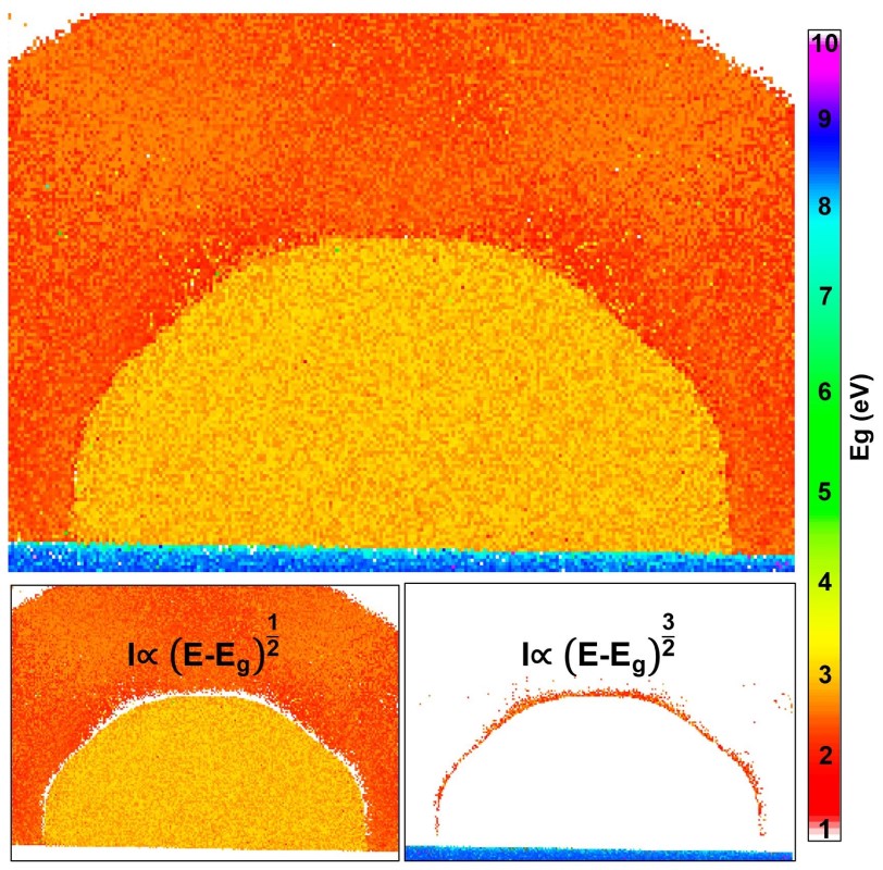
ICN2 researchers were able to map the evolution of the energy bandgap of the nanowires (at their cross-section) down to sub-nanometer scale thanks to a new methodology that they developed, which is based on valence electron energy-loss spectroscopy (VEELS) performed in a mono-chromated STEM. Electron energy loss spectroscopy (EELS) and valence EELS (or VEELS) are techniques currently used in transmission electron microscopes for measuring the ionization losses suffered by the electron beam. The second one provides both high energy and high spatial resolution and thus it is particularly suited for bandgap measurements.
The authors of this work could reveal the effects of the interfacial strain on the electronic properties of the heterostructured material and demonstrated a direct to indirect bandgap transition at the 3-5 nanometer interface region due to the large strain accumulation observed at the atomic scale. Their new VEELS methodology combines computer modeling and simulations with accurate data analysis.
This study not only provides interesting results about these specific semiconductor hetero-nanowires grown with a horizontal technique, but also proves that an atomic-scale accurate analysis of nanostructured materials and their interfaces is key to understanding and controlling their properties. This will result in improved ability to control and tune the behaviour of the electronic, photonic or quantum devices in which such structures will be used, such as nanoengineered circuits and networks.
This research was coordinated by ICREA Prof. Jordi Arbiol, leader of the ICN2 Advanced Electron Nanoscopy Group. First authors of the paper are Dr Sara Martí-Sanchez and Marc Botifoll, postdoctoral researcher and PhD student, respectively, in Prof. Arbiol’s group. Nanowire samples were grown at the Weizmann Institute of Science (Rehovot, Israel), at Prof. Ernesto Joselevich’s group. VEELS low loss simulations were carried out at ICFO under supervision of Prof. Javier García de Abajo. Part of the STEM and electron energy loss spectroscopy (EELS) analyses were performed at the SuperSTEM by Prof. Quentin Ramasse.
Reference article:
Sara Martí-Sánchez, Marc Botifoll, Eitan Oksenberg, Christian Koch, Carla Borja, Maria Chiara Spadaro, Valerio Di Giulio, Quentin Ramasse, F. Javier García de Abajo, Ernesto Joselevich & Jordi Arbiol, Sub-nanometer mapping of strain-induced band structure variations in planar nanowire core-shell heterostructures. Nat Commun 13, 4089 (2022). DOI: https: 10.1038/s41467-022-31778-3