Nanofabrication facility - Case studies
Case studies
Nanofabrication has the power to influence a vast number of academic fields and produce immediate and disrupted changes in industries such as hospitals and health care, right through to energy harvesting and food production.
The key to progress in nanoscience and nanotechnology relies on the ability to design and fabricate samples for the experimental work. In order to understand the fundamentals of science, fabrication of nanostructures in a variety of materials with accuracy in the nano-meter scale and sometimes in the molecular scale is essential. To this extent ICN2 Nanofabrication Facility has built the dynamic environment to combine materials, processes and characterisation techniques to efficiently delivery devices for both fundamental and prototyping research purposes. Our institutional high-impact and multidisciplinary research activities guarantee’s the success for high-quality, innovative and excellent research outcomes.
Pioneering Expertise
ICN2 Nanofabrication Facility has been pioneering advanced nanofabrication technologies concealing applications from the molecular up to the macro world, engaging its research to understand and solve fundamental scientific problems. Our highly skilled personnel together with our state of the art infrastructure addresses all the requirements for excellence and ground-breaking results. The expertise at ICN2 is particularly relevant in hybrid technologies applied to the nanoscale with relevant focus on the application areas of biosensors, photonics, nanomedicine, energy and drug delivery. We have highlighted projects in some of these areas in a series of case studies.
Browse some examples
Molecular Factory
-
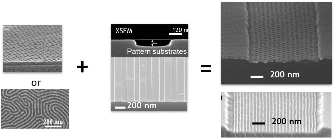
Scaling has driven the microelectronics industry for over 40 years and revolutionised information and communication technologies. Maintaining progress by the introduction of new technologies is an important challenge as extensions to UV-lithography may limit the feature size realizable at acceptable costs. ICN2 NIL Platform and P2N group have developed a novel nanofabrication technique to realize sub 10 nm domains in a high throughput manner. In particular direct self-assembly of block copolymers with chemically designed polymer films have been coupled to a nanoimprint method to generate topographically ordered substrates to define precise pattern alignment and orientation. This nano-patterning methodology has been developed for the creation of sub 10 nm feature size patterns over large areas (up to 8”). Both line and pillar patterns have been realized. These patterns were integrated into processes to allow pattern transfer to a substrate to create arrays of nanostructures of silicon, copper and germanium.
Dynamic surfaces
-
An alternative method for generating free-formed dynamic surfaces has been developed by ICN2 NIL Platform in close collaboration with P2N group. The novel micro/nano manufacturing technique utilized to generate hierarchical two-level micro and nano patterned structures with amazing water repelling properties. In particular our surfaces exhibit super-hydrophobic (>160o) and self-cleaning properties (CA<10o), while engineering the surface topography one could precisely control the wetting conditions delivering dynamic effects.


Antibacterial surfaces
- ICN2 NIL Platform is investigating the formation of micro/nano topographies on bio-degradable polymer films with dimensions comparable to those of cells or biological macromolecules. Nanoimprint lithography, a novel method of pattern replication in polymers, has been used for the production of features ranging from tens of micrometers, covering areas up to 1 cm2, down to hundreds of nanometers. The bacterial attachment patterns of some bacteria, highlighted that the nano-patterned biofilm can reduce the propensity for the bacteria to attach to the surface, with a greater bactericidal being demonstrated activity against the Staphylococcus aureus cells.


Conductive electrodes for OPV
- ICN2 NIL platform has engineered an entirely new process for optimizing current collection of Ag grids made by a combination of nanoimprint lithography and inkjet printing techniques. In particular the replacement of the ITO electrode in an organic solar cell configuration was replaced by an 90% embedded Ag grid structure. This feasible, low-cost and potentially R2R compatible technique demonstrated an evident enhancement in the fill factor (FF > 60 %) of the solar cell device.


Light Manipulation
- Next generation optical devices have to meet specific requirements such as, low cost, small dimensions, long-term stability, low energy consumption and manufacturability. Over the last years several research efforts have been placed to investigate physical methods to improve the external efficiency of organic LED’s. ICN2 P2N group and NIL platform have pioneered a methodology of increasing the efficiency of LED devices by modifying the spontaneous emission characteristics. In particular the introduction of an artificial photonic band gap geometry in the active material of the LED device generates the conditions for the modification of the spontaneous emission rate, enhancing it up to 3 times in comparison to the unpatterned active material.

Dimensional Nanometrology
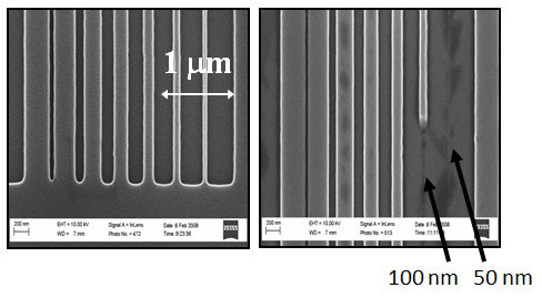
- Non-invasive, high-speed and in-line dimensional metrology systems are a prerequisite for advanced nano-manufacturing lines. ICN2 NIL platform in close collaboration with P2N group have developed an optical prototype measuring tool based on a diffractometry to carry out in-line quality control during the roll-to-roll nanoimprint lithography process. The metrology tool measures diffractograms at normal incidence, reflection geometry to gain fast, non-invasive information of defects and the critical dimensions from the replicated structures with a sub-50 nm resolution capability.
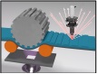
Graphene device technology for in vitro experiments
- ICN2 AEMD group has dedicated efforts in the electrical and electrochemical characterization in vitro of the graphene based field-effect transistors and electrodes. Therefore they fabricate arrays of devices (80x80 micro graphene transistors/ electrodes) with different geometries such as width to length ratio and different contact types on rigid substrates such as SiO2 or Pyrex 4-inch wafers. They have developed a home-made electronic system and software which allows the simultaneous characterization of such devices.

Graphene flexible devices for preclinical in vivo assessment
- Pictures below show the flexible devices for preclinical in vivo assessment developed by ICN2 AEMD group. The picture shows a 4-inch wafer with the neural sensors on a flexible biocompatible polymer before the peeling from the rigid sacrificial substrate. These types of graphene sensors are used in an in vivo experiment by placing the tip of the probe on top of a rodent cortex to measure the brain activity.
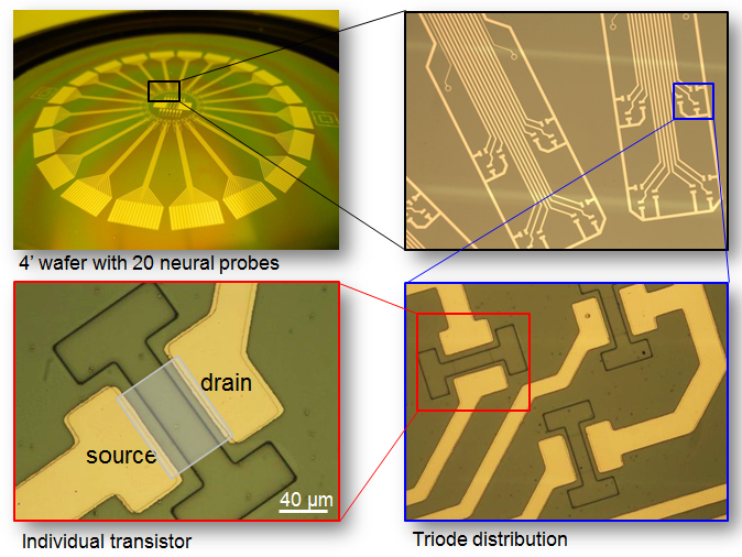
Neural Implants
- ICN2 AEMD group fabricate neural implants with different physiological application. Some of the flexible graphene based devices are used for cortical recordings of neural activity (micro-electrocorticograms (uECoG)). Other devices are intended to be inserted in the cortex in order to measure the activity in the different levels of the cortex. Some others are probes to record and perform deep brain stimulation.
Metamaterials
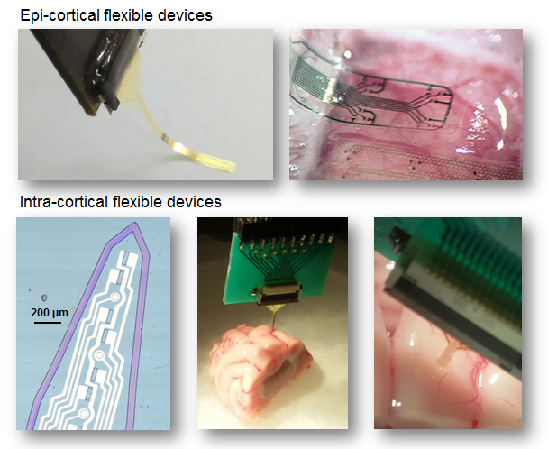
- ICN2 NB2A Group in close collaboration with MN Group have developed a novel nanofabrication methodology, which enables the generation of high aspect-ratio nanostructure arrays with height gradients in arbitrary directions by a single and fast etching process. Based on metal-assisted chemical etching using a catalytic gold layer perforated with nanoholes, they have demonstrated how nanostructure arrays with directional height gradients can be accurately tailored by: (i) the control of the mass transport through the nanohole array, (ii) the mechanical properties of the perforated metal layer, and (iii) the conductive coupling to the surrounding gold fi lm to accelerate the local electrochemical etching process. The proposed technique, enabling 20-fold on-chip variation of nanostructure height in a spatial range of a few micrometers, offers a new tool for the creation of novel types of nano-assemblies and metamaterials with interesting technological applications in fields such as nanophotonics, nanophononics, microfluidics or biomechanics.(Ref. M.A.Otte et al. Small 2015,11, No.33, 4201-4208)
Spintronics
- ICN2 PEN group has proved the electrical detection of spin precession in freely-suspended graphene spin valves. The devices are fabricated with a single electron-beam-resist process that minimizes the fabrication steps and the number of (aggressive) chemicals used. The pictures below show SEM images of a suspended graphene FET device, used for spin transport studies (Ref. Neumann et al. Small 2013, 9, No. 1, 156–160).
